English


| Quantity: | |
|---|---|
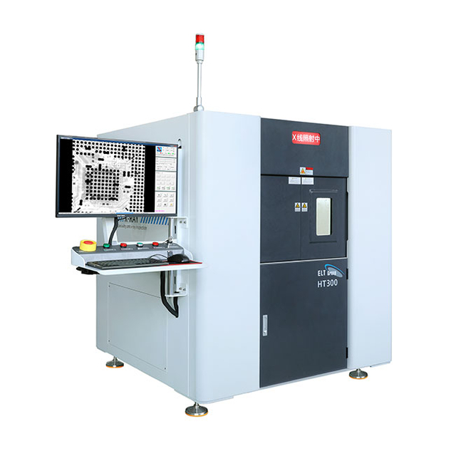
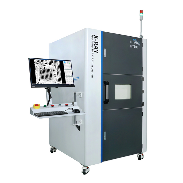
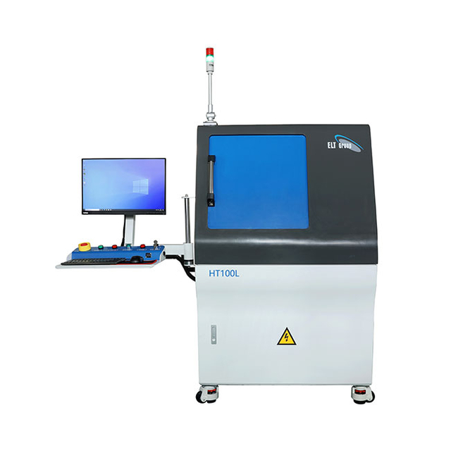
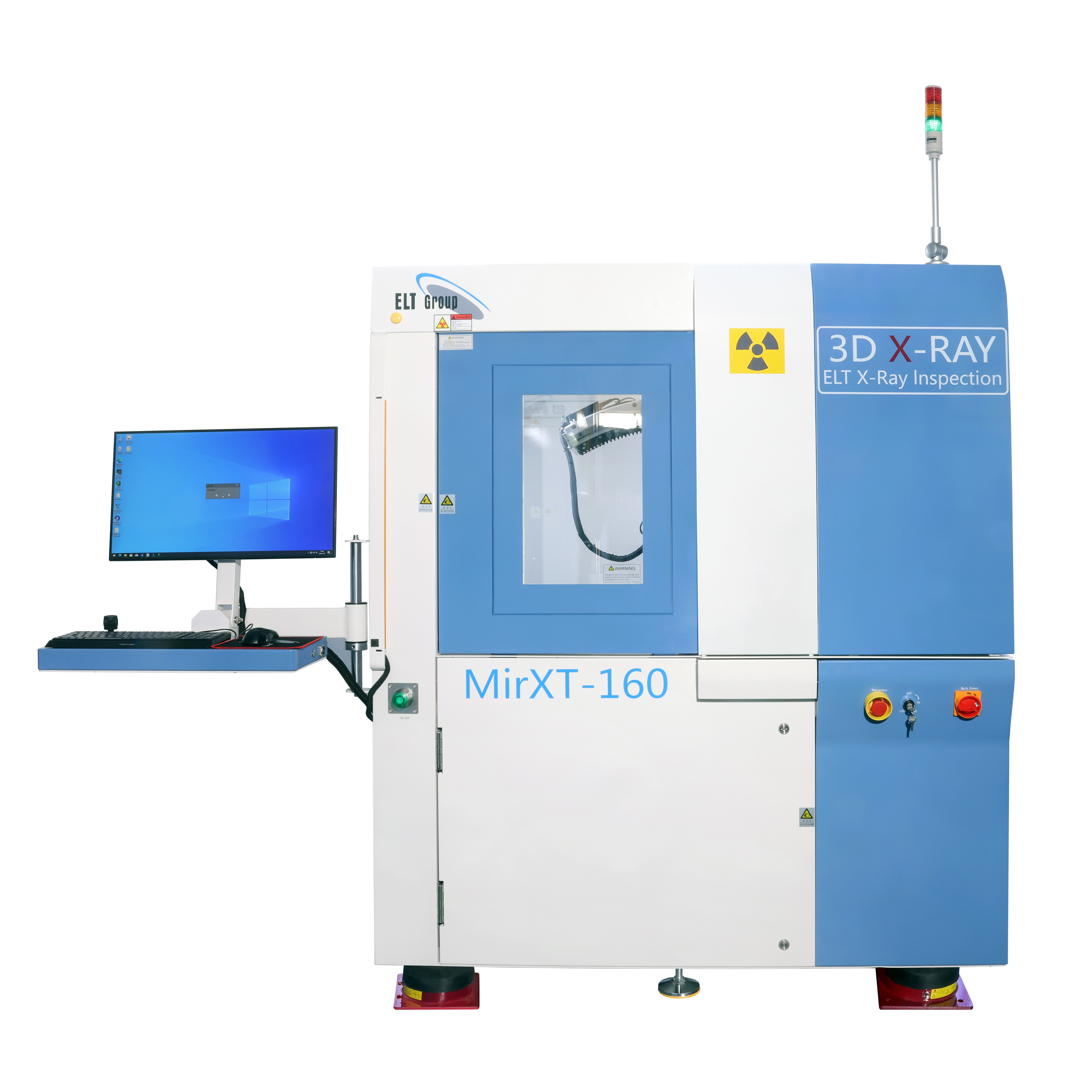
3D X-ray CT Inspection System For Semicon/Electronics Inspection--MirXT-160 ![]()
The 3D X-ray inspection system MirXT-160 is specially tailored for wafer technology, SMT, packaging inspection, semiconductor and laboratory applications. The equipment is used to detect solder/tin voids and bonding wires generated in the SMT/semiconductor manufacturing process in the electronic industry. Packaging defects such as offset, wire cross short circuit, flip-chip solder ball virtual soldering, flip-chip solder ball short circuit, wire breakage, wire detachment, etc.
1. Modular design, user-customized system
2. Multi-axis motion control system enables clear detection from different angles
3. Automatic real-time navigation chart and x-ray image navigation chart function
4. Specially designed OVHM module, the detector can rotate 360 degrees horizontally and tilt 70 degrees
5. Ultra-high-speed, high-definition CT images
6. Product process programming, with automatic detection function, 5-axis interpolation function, visual CNC detection, and unlimited point editing
7. Digital real-time image processing technology, professional configuration HDR image enhancement technology functions
8. Maximum tube voltage: 160KV, maximum power 20W
9. Geometric magnification up to 2100x, total magnification up to 23000x
10. The smallest detection capability can reach: 0.35 micron
11. ovhm technology High magnification bevel detection
![]()
![]()


![]()

Note: The above information only represents general descriptions and characteristics, which may change with technological advancement and equipment upgrades. Specific parameters are subject to the final agreement.
3D X-ray CT Inspection System For Semicon/Electronics Inspection--MirXT-160 ![]()
The 3D X-ray inspection system MirXT-160 is specially tailored for wafer technology, SMT, packaging inspection, semiconductor and laboratory applications. The equipment is used to detect solder/tin voids and bonding wires generated in the SMT/semiconductor manufacturing process in the electronic industry. Packaging defects such as offset, wire cross short circuit, flip-chip solder ball virtual soldering, flip-chip solder ball short circuit, wire breakage, wire detachment, etc.
1. Modular design, user-customized system
2. Multi-axis motion control system enables clear detection from different angles
3. Automatic real-time navigation chart and x-ray image navigation chart function
4. Specially designed OVHM module, the detector can rotate 360 degrees horizontally and tilt 70 degrees
5. Ultra-high-speed, high-definition CT images
6. Product process programming, with automatic detection function, 5-axis interpolation function, visual CNC detection, and unlimited point editing
7. Digital real-time image processing technology, professional configuration HDR image enhancement technology functions
8. Maximum tube voltage: 160KV, maximum power 20W
9. Geometric magnification up to 2100x, total magnification up to 23000x
10. The smallest detection capability can reach: 0.35 micron
11. ovhm technology High magnification bevel detection
![]()
![]()
![]()
Note: The above information only represents general descriptions and characteristics, which may change with technological advancement and equipment upgrades. Specific parameters are subject to the final agreement.